Amid Intel's deals, Intel Foundry remains notably absent — 18A and 14A are on the way, but success isn't guaranteed
DARPA’s experiment comes as the semiconductor industry itself pivots toward multi-chip packaging. Apple, Intel, AMD, Nvidia, and TSMC all rely on some form of advanced integration to extend performance gains, now that transistor scaling alone can no longer keep pace with demand.
Intel has invested heavily in this direction through its IDM 2.0 strategy, pairing new fabrication nodes with technologies like Foveros and EMIB, which connect multiple dies within one package. In 2024, Intel opened its $3.5 billion advanced packaging hub in New Mexico, capable of bonding chiplets made on different process nodes. The company’s packaging expertise has already landed it a $5 billion collaboration with Nvidia , which will use Intel’s Foveros technology to combine GPU and CPU chiplets on a single package.
AMD and TSMC, meanwhile, have taken chiplet integration mainstream. AMD’s MI300A accelerator integrates thirteen chiplets — CPUs, GPUs, I/O, and stacked HBM3 memory — inside one module. TSMC provides the 2.5D and 3D packaging infrastructure that underpins AMD, Apple, and Nvidia’s flagship products through its CoWoS and SoIC platforms. Apple’s M1 Ultra uses TSMC CoWoS to fuse two M1 Max chips at a combined 2.5 TB/s inter-chip bandwidth.
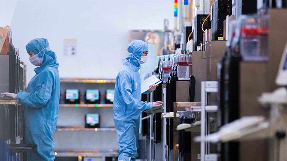
DARPA’s NGMM differs in both scope and purpose. Commercial packaging focuses on connecting silicon dies for higher performance or memory bandwidth. The Austin fab targets heterogeneous integration across materials and device classes, assembling sensors, power amplifiers, and logic circuits that would never share a wafer in traditional production. It also aims to provide open access, allowing small companies and researchers to experiment without the massive entry costs of a private fab.
The initiative dovetails with a wider federal strategy. While NGMM is funded by the Department of Defense, it complements the CHIPS and Science Act’s National Advanced Packaging Manufacturing Program, an effort to expand domestic R&D infrastructure for chip assembly and test. Together with Intel’s expansions and Amkor’s planned Arizona facility — which will package Apple’s U.S.-made chips from TSMC’s Phoenix fab — NGMM represents a three-pronged attempt to rebuild a complete onshore supply chain.
High-performance computing and AI chips are already constrained by thermal density and memory bandwidth, areas where 3DHI could offer breakthroughs. Integrating logic and memory vertically could shorten signal paths and reduce power, while new materials such as microfluidic cooling films or on-package photonics could allow stacked layers to operate without overheating.
For AI systems, that means faster interconnects and lower latency between compute units, which is an urgent need as model sizes climb into the trillions of parameters . For defense, it promises more compact, power-efficient electronics for radar, imaging, and communications, all designed and built domestically.
The Austin fab also serves a longer-term industrial goal of proving that a low-volume, high-complexity foundry can be financially sustainable. Once DARPA’s five-year funding runway ends, TIE plans to operate as an independent commercial entity supported by government contracts and specialty manufacturing orders. The viability of that model will depend on whether its unique capabilities can attract a steady pipeline of customers in the aerospace, computing, and energy sectors.
Ultimately, NGMM reflects a growing consensus that semiconductor innovation is now concerned with what’s above the wafer, not within it. The Austin facility’s success will depend heavily on execution, because building reproducible processes for 3DHI is far more complex than packaging homogeneous silicon dies — and creating a business from that foundation is harder still. Yet if it delivers on even part of its promise, NGMM could establish a new center of gravity for U.S. semiconductor research and manufacturing complements, rather than competes with, traditional fabs.
Follow Tom's Hardware on Google News , or add us as a preferred source , to get our latest news, analysis, & reviews in your feeds.
Luke James Social Links Navigation Contributor Luke James is a freelance writer and journalist. Although his background is in legal, he has a personal interest in all things tech, especially hardware and microelectronics, and anything regulatory.
Key considerations
- Investor positioning can change fast
- Volatility remains possible near catalysts
- Macro rates and liquidity can dominate flows
Reference reading
- https://www.tomshardware.com/SPONSORED_LINK_URL
- https://www.tomshardware.com/darpa-invests-1-4-billion-to-build-texas-foundry-for-next-gen-3d-chip-integration#main
- https://www.tomshardware.com
- Fall Into Gaming With 20+ Titles Joining GeForce NOW in November
- Five convicted for helping North Korean IT workers pose as Americans and secure jobs at U.S. firms — over 240 companies were victimized by the scam
- Microsoft Windows boss posts lackluster response to ‘agentic OS’ backlash — Microsoft is working to address broad problems with the OS
- Microsoft to appeal ruling in favor of reselling perpetual Windows licenses — UK Competition Court says fineprint holds no ground as judges throw out company's
- Manufacturers reportedly delaying launch of new memory modules due to massive price crunch — products slated for 4Q25 now expected to arrive in 2026
Informational only. No financial advice. Do your own research.
