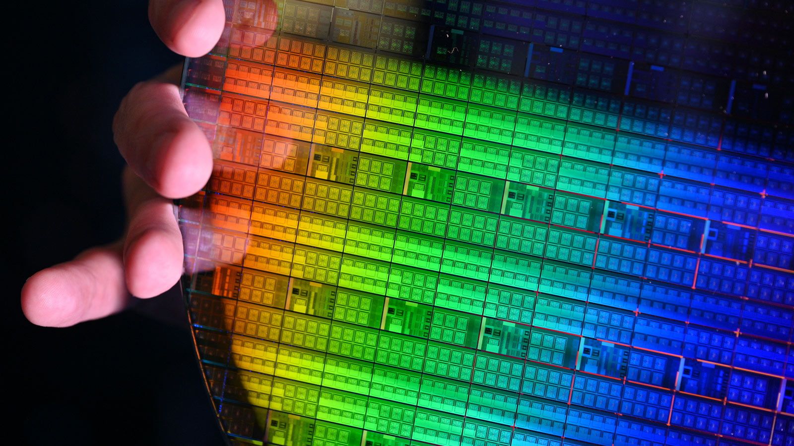
“Even when we extrapolate the best-case scenario for chip production from our suppliers, it is still not enough,” Musk told the audience. “So, I think we may have to do a Tesla TeraFab. It is like [TSMC’s] Giga[fab] but way bigger. I cannot see any other way to get to the volume of chips that we are looking for, so I think we are probably going to have to build a gigantic chip fab. It’s gotta be done.”
It costs leading-edge chipmakers billions of dollars to develop a fabrication process and tens of billions to build a single fab with a 20,000 WSPM capacity capable of making chips on a state-of-the-art process technology.
Rapidus — Japan’s first new chipmaker with plans to build chips on advanced nodes in decades — estimates that it needs around ¥5 trillion (about $32 billion) in total investment to develop a process technology and build a fab capable of commercial production of 2 nm-class chips in 2027. While we can only applaud this ambitious project, it remains to be seen whether becoming a leading chipmaker from scratch is possible in the 2020s and with leading-edge nodes.
Developing a new process technology from scratch is a particularly complex, multidisciplinary endeavor that takes 5 or more years these days, from inception to yield ramp. A development cycle of a fabrication technology begins with pathfinding, materials research, transistor structure development, and then running countless TCAD simulations to model doping, strain, and leakage for a new transistor.
Rapidus has licensed its 2nm GAA transistor structure from IBM, but it is also possible to license a chunk of similar technologies from imec and CEA-Leti, public-private R&D institutes. But while it is hard to overestimate the importance of the right transistor structure, this is only the start.
Once transistor technology is complete, engineers build thousands of tightly coupled process steps organized into FEOL, MOL, and BEOL modules — covering transistor formation, interconnects, and metallization. Each of these steps demands atomic-level precision in deposition, etch, lithography, and anneal. Tuning those steps (each with hundreds, if not thousands, of parameters) for manufacturability, uniformity, reliability, defectivity, power, and performance requires decades of engineering experience and time from the team. At this point, technology providers like IBM, Imec, or CEA-Leti cannot really help.
Once each deposition, etch, implant, lithography, and anneal step is stable in isolation, engineers start combining modules (e.g., transistor gate stack and source/drain) on test wafers and tune their sequencing and temperature budgets to prevent cross-contamination or material degradation. This is essentially when the ordered stack of hundreds of steps that define the node — the process flow — takes shape. Again, these integration recipes are not available for licensing from R&D companies or institutes.
After device performance, power, and yield meet targets, the process must be made design-usable by generating PDKs, SPICE models, verified standard-cell libraries for EDA tools, and IPs for chip designers. At the same time, engineers begin implementing the fabrication process in actual fabs and production lines. That implementation and setting the right parameters for equipment is another challenge that demands experience, not something money can buy.
Finally, fabs must achieve high yields in mass production, which is a hard, long, and iterative process involving plenty of experienced engineers. Can this all be done from scratch in a mere five years by a newcomer? Rapidus will show in 2027.
Follow Tom's Hardware on Google News , or add us as a preferred source , to get our latest news, analysis, & reviews in your feeds.
Anton Shilov Social Links Navigation Contributing Writer Anton Shilov is a contributing writer at Tom’s Hardware. Over the past couple of decades, he has covered everything from CPUs and GPUs to supercomputers and from modern process technologies and latest fab tools to high-tech industry trends.
logainofhades In other words Jensen doesn't want any potential competition. Reply
Gururu I don't doubt Musk can do it with the sheer wealth he commands. Reply
Key considerations
- Investor positioning can change fast
- Volatility remains possible near catalysts
- Macro rates and liquidity can dominate flows
Reference reading
- https://www.tomshardware.com/tech-industry/semiconductors/SPONSORED_LINK_URL
- https://www.tomshardware.com/tech-industry/semiconductors/elon-musk-says-terafab-chip-fab-may-be-the-only-answer-to-teslas-colossal-ai-semiconductor-demand-nvidia-ceo-jensen-huang-warns-against-extremely-hard-challenge#main
- https://www.tomshardware.com
- Explosive AI buildout brings into question water supply concerns — exploring how data centers could curb water demands
- Popular camera company dishes out gold keycaps worth up to $45,000 to top employees — more than 50 prizes given out by Insta360
- Hard drives on backorder for two years as AI data centers trigger HDD shortage — delays forcing rapid transition to QLC SSDs
- The world's ‘tiniest GPU’ heads to production — 200,000-transistor TinyGPU v2.0 can render gamepad-manipulated 3D images with up to 1K triangles in real-time
- NVIDIA AI Physics Transforms Aerospace and Automotive Design, Accelerating Engineering by 500x
Informational only. No financial advice. Do your own research.
