Researchers demonstrate FeFET-based 3D NAND cells with near-zero pass voltage and up to five bits per cell.
When you purchase through links on our site, we may earn an affiliate commission. Here’s how it works .
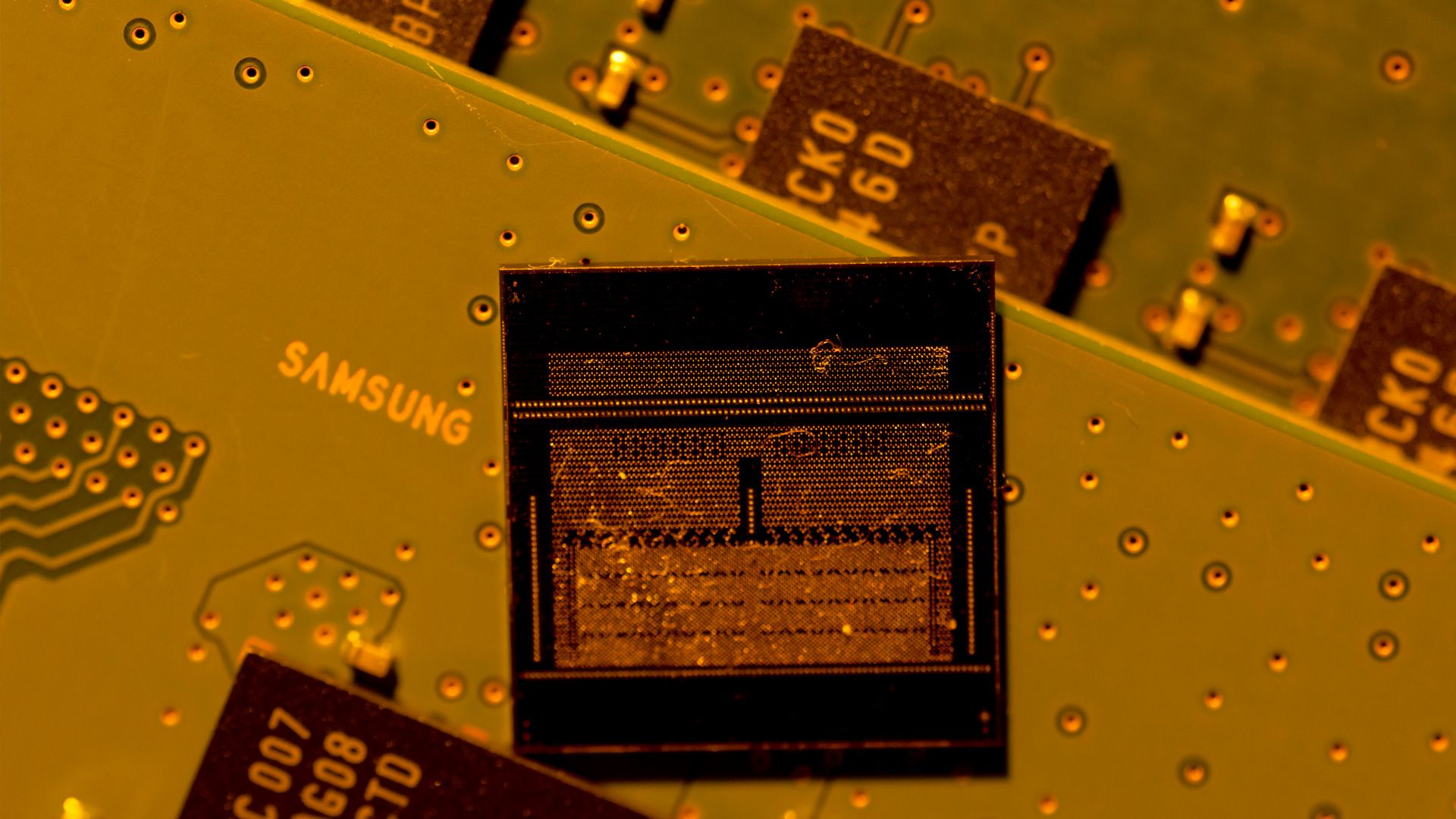
(Image credit: Getty Images/Bloomberg) Samsung researchers have published a detailed account of an experimental NAND architecture that aims to cut one of the technology’s largest power drains by as much as 96%.
In modern NAND, the stack of wordlines running through each vertical string must be biased with a pass voltage every time a cell is read or programmed. As layer count increases , so too does that overhead, and it now represents a significant share of total array power as a result of higher layer counts. The Samsung teams argue that a ferroelectric transistor with a wide memory window and a maximum threshold voltage pushed below zero can support multi-level operation without the high Vpass that charge-trap NAND relies on to avoid disturb.
Next-gen MRAM breakthrough can flip bits at SRAM-rivalling speeds with low power consumption
Researchers achieve breakthrough integration of 2D materials on standard silicon chips
SK hynix unveils AI NAND strategy, including gargantuan petabyte-class QLC SSDs — ultra-fast HBF and 100M IOPS SSDs also in the pipeline
They demonstrate this first in planar arrays operating at up to five bits per cell and then in a short four-layer vertical string designed to mimic 3D NAND geometry. The central gates in that structure measure 25 nanometres, similar to current commercial devices. The group defines a NAND-specific energy metric that combines the dominant contributions from wordline capacitance and the internal charge pumps that generate the high voltages required for reads and writes.
By modelling those costs for a full stack, the researchers estimate that a 286-layer device based on the ferroelectric design could reduce combined program and read energy by about 94% compared with a conventional charge-trap stack of the same height. At 1,024 layers, the reduction passes 96% as the lower pass voltage sharply lowers the work done by the charge pumps.
The experiments also cover retention and cycling limits. In planar form, the ferroelectric cells support a wide memory window and demonstrate five-level programming, although endurance at that density is modest. A PLC-class configuration holds for a few hundred cycles, while QLC-equivalent use approaches a thousand at both room temperature and 85 °C. The authors note that further development of program-inhibit schemes and negative-voltage generation will be required before a full 3D array could be qualified for production. They also point out that the oxide channel’s behaviour under high-temperature stress remains a key area for follow-up work.
As of now, there is nothing to suggest that Samsung plans any product announcements based on this work. Instead, the study is being framed as a piece of foundational research, which itself requires further development, for potential low-power NAND generations beyond the current charge-trap roadmap.
Get Tom's Hardware's best news and in-depth reviews, straight to your inbox.
Key considerations
- Investor positioning can change fast
- Volatility remains possible near catalysts
- Macro rates and liquidity can dominate flows
Reference reading
- https://www.tomshardware.com/tech-industry/semiconductors/SPONSORED_LINK_URL
- https://www.tomshardware.com/tech-industry/semiconductors/samsung-researchers-publish-96percent-lower-power-nand-design-based-on-ferroelectric-transistors#main
- https://www.tomshardware.com
- The Largest Digital Zoo: Biology Model Trained on NVIDIA GPUs Identifies Over a Million Species
- Taiwan hits Japanese firm with indictment in TSMC data theft saga — Tokyo Electron charged with failing to prevent its staff from stealing trade secrets
- Save $620 on high-end Core Ultra 9 285K and motherboard bundle with 32GB of RAM — get over $1,500 in gear for less than $800
- Samsung touts 96% lower-power NAND design — researchers investigate design based on ferroelectric transistors
- Enthusiast adds OCuLink port to Framework 16 Laptop — offering PCIe 4.0 x8 bandwidth for big GPU performance gains
Informational only. No financial advice. Do your own research.
