TSMC, Samsung, and Intel shore up support with ASML to deploy larger High-NA EUV photomasks — 6×12-inch photomask transition may take years despite unified effo

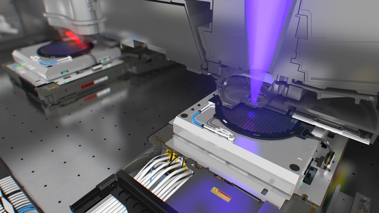
Perhaps the biggest changes would be required from ASML. Its High-NA EUV scanners would need modifications or a redesign to accept, clamp, move, and position the substantially larger reticles with the extreme precision r…

TSMC, Samsung, and Intel shore up support with ASML to deploy larger High-NA EUV photomasks — 6×12-inch photomask transition may take years despite unified effo

Perhaps the biggest changes would be required from ASML. Its High-NA EUV scanners would need modifications or a redesign to accept, clamp, move, and position the substantially larger reticles with the extreme precision r…

Intel surpasses one million High-NA EUV wafers processed, outpaces the rest of the industry combined — company also trailblazing giant 6×12 photomasks to speed

Moving from 6×6-inch to 6×12-inch photomasks would require substantial changes across the existing mask ecosystem, including mask blanks and deposition, etching, inspection and metrology, cleaning, pellicles, mask writer…

Intel surpasses one million High-NA EUV wafers processed, outpaces the rest of the industry combined — company also trailblazing giant 6×12 photomasks to speed

Moving from 6×6-inch to 6×12-inch photomasks would require substantial changes across the existing mask ecosystem, including mask blanks and deposition, etching, inspection and metrology, cleaning, pellicles, mask writer…