
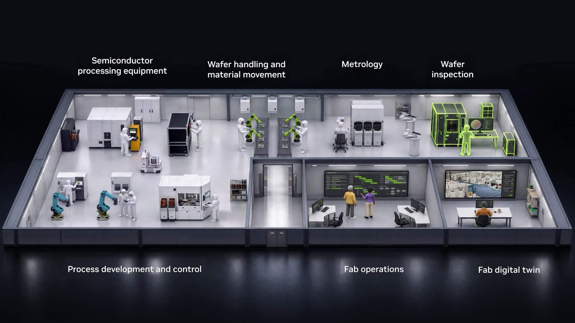
And digital twins let teams test changes in a virtual environment before committing to physical trials.
Together, these capabilities describe an AI-defined fab: a semiconductor manufacturing factory where AI helps engineers optimize processes, catch problems earlier and make better decisions across the full manufacturing chip lifecycle. Engineers direct the work and make decisions based on their expertise while spending less time waiting for answers.
Accelerated computing doesn’t just speed up individual calculations — it changes how many alternatives engineers can test before committing.
Multiphysics simulations model interactions among physical effects, such as heat transfer, electrical behavior and mechanical stress.
Using the NVIDIA cuDSS library, multiphysics simulation software provider COMSOL is accelerating such simulations for semiconductor manufacturing by up to 10x. This helps engineers optimize equipment and processes, compare alternatives and decide which changes to test physically.
Applied Materials and NVIDIA are collaborating to accelerate atomic-scale materials discovery and process development. By integrating NVIDIA cuDSS, Applied’s Ginestra simulation platform runs up to 10x faster than CPU-only approaches. And with NVIDIA PhysicsNeMo, Applied’s ACE+ multiphysics platform delivers topography simulations up to 35x faster.
In some cases, acceleration doesn’t just shorten the calculation — it enables it altogether. Computational lithography — which defines how circuit patterns are printed onto silicon — involves calculations too intensive to complete on CPU at production scale. Siemens is integrating NVIDIA cuLitho into its Calibre lithography software, delivering up to 17x acceleration on key simulation workloads. That expands what engineers can verify before a wafer goes to print.
As such, faster calculations can help researchers explore material behavior and reaction pathways that influence next-generation semiconductor processes.
In addition to accelerating simulations, AI trained on physics can predict how materials and processes will behave — without running a full simulation each time.
The payoff is most visible in complex calculations that are expensive even on accelerated hardware.
Plasma — the electrically charged gas used in semiconductor etch processes — is one example. Modeling plasma behavior requires solving equations that capture how electrical, chemical and thermal processes interact, making repeated simulation costly. NVIDIA PhysicsNeMo can assist in reducing plasma-prediction simulation time from days to as little as milliseconds.
Lam Research intends to integrate NanoVDB into its advanced semiconductor process modeling platform SEMulator3D, part of the company’s Semiverse Solutions family of virtual products. The addition of NanoVDB is expected to accelerate select wafer-etch modeling by up to 30x.
Engineers turn analyses into decisions — revising a design, investigating a test failure, adjusting a production process and more.
AI agents can help carry out the steps between those decisions.
Key considerations
- Investor positioning can change fast
- Volatility remains possible near catalysts
- Macro rates and liquidity can dominate flows
Reference reading
- https://blogs.nvidia.com/blog/ai-semiconductor-fabs/#primary
- https://blogs.nvidia.com/blog/author/timothycosta/
- https://blogs.nvidia.com/blog/ai-semiconductor-fabs/#disqus_thread
- NVIDIA Announces New Planned Investments in Korean Startups at the MSIT-NVIDIA AI Startup Partnership Forum
- Vera Delivers the Best of Both Worlds: Highest Throughput and Fastest Agents
- NVIDIA Announces New Planned Investments in Korean Startups at the MSIT-NVIDIA AI Startup Partnership Forum
- Nvidia released its 8800 GTX GPU 20 years ago today, celebrates with Steam game homage
- Grab 32GB DDR5 for $371 in this Newegg RAM bundle with the 9800X3D, $70 less than buying it separately
Informational only. No financial advice. Do your own research.