
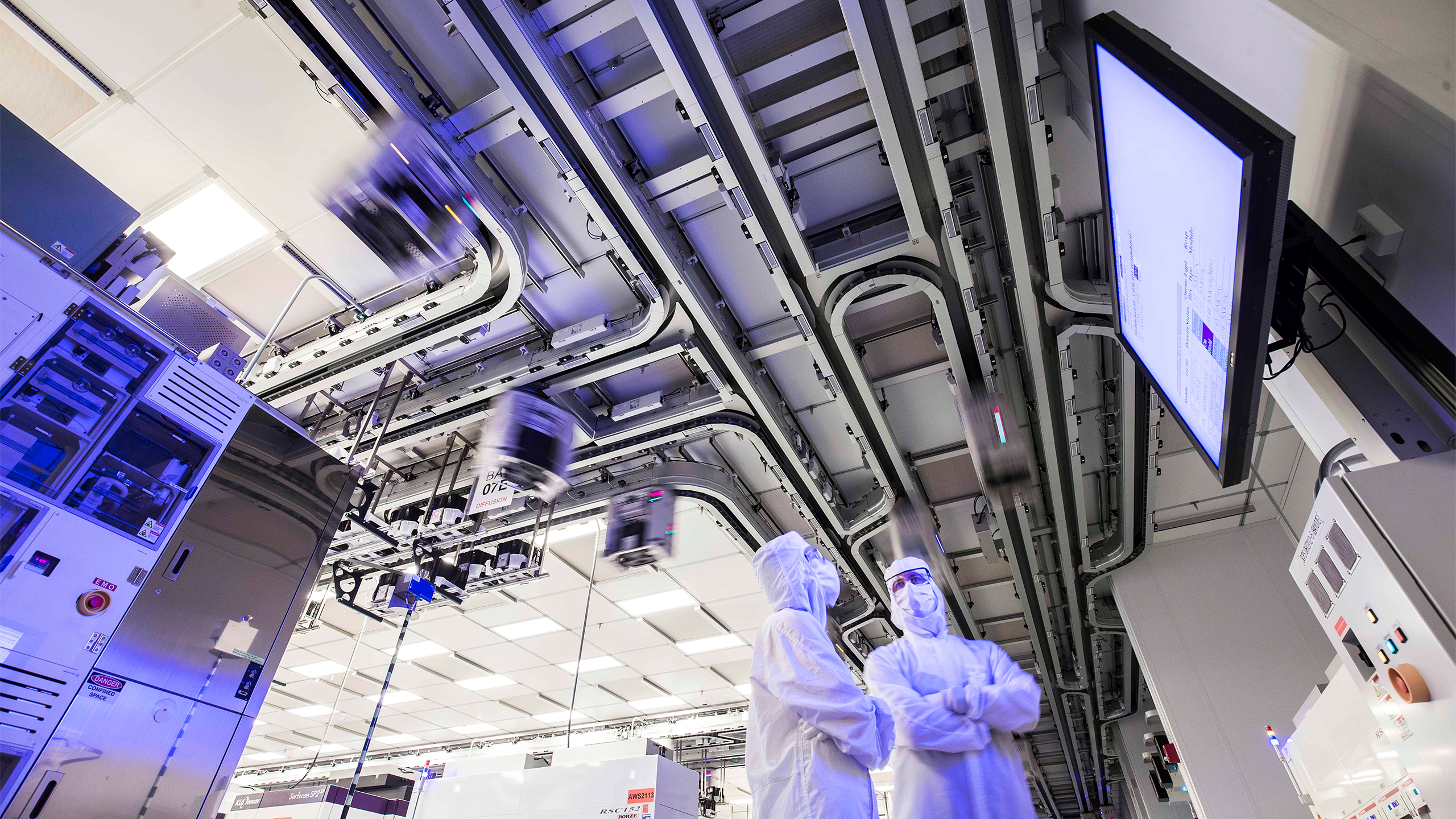
When GlobalFoundries claims 2X 'digital performance' comparable to that of 7nm-class technologies, it doesn't reveal whether it means transistor switching speed, standard cell performance, achievable operating frequency, or something else. In addition, the company promises more than twice the logic density of its first-generation FDX technology, although the firm does not reveal any actual numbers. Consequently, it is unclear how FDX Fusion will compare with established 7nm-class FinFET technologies, which offer mature defect density and yields, plenty of supply, an established design ecosystem, and predictable pricing among other things, in terms of transistor density, performance, power consumption, and production costs. While CEA-Leti's comment seems promising, actual numbers are always better.
The very fact that GF's FDX Fusion planned 2028 introduction will come roughly nine years after the originally anticipated first 12FDX tape-outs illustrates significant technological and/or financial difficulties associated with the development of FD-SOI beyond the 22nm generation. So, while GlobalFoundries' FDX Fusion initiative certainly looks promising, it remains to be seen how that is going to play out for the contract chipmaker and its clients.
For now, the lineup of supporters from the automotive and industrial sectors — BMW, Bosch, Infineon, NXP, Siemens, and Tesla — certainly looks promising. But what about other applications? While established semiconductor companies such as Infineon and NXP already possess extensive processor IP portfolios, smaller fabless developers could benefit from GF’s MIPS and ARC processor cores, RISC-V expertise, and custom chip design capabilities, which could substantially reduce the cost and complexity of developing specialized SoCs. Still, to attract a broader range of chip developers, GlobalFoundries will need a mature ecosystem of EDA tools, standard-cell libraries, memory compilers, interface IP, and other silicon-proven building blocks. These are the things that GlobalFoundries has not touched upon in its press release.
Follow Tom's Hardware on Google News , or add us as a preferred source , to get our latest news, analysis, & reviews in your feeds.
Anton Shilov Social Links Navigation Contributing Writer Anton Shilov is a contributing writer at Tom’s Hardware. Over the past couple of decades, he has covered everything from CPUs and GPUs to supercomputers and from modern process technologies and latest fab tools to high-tech industry trends.
bit_user It's nice to see they're getting the ball rolling on process improvements, at least. I hope it won't be nearly as long before their next node introduction. Reply
thestryker As far as I'm aware they haven't acquired any EUV machines so it's probably a safe bet that the node won't match existing "7nm" nodes. I believe all of the nodes on the market with similar application are based on 20nm or higher original nodes though so there's definitely a lot of room for improvement. Given that their aborted "12" node was based on their 14nm process it has always made me wonder if there was something simply unsuitable which would require a purpose built node. It definitely sounds like this forthcoming node isn't going to be built directly off of anything existing. Reply
Key considerations
- Investor positioning can change fast
- Volatility remains possible near catalysts
- Macro rates and liquidity can dominate flows
Reference reading
- https://www.tomshardware.com/tech-industry/semiconductors/SPONSORED_LINK_URL
- https://www.tomshardware.com/tech-industry/semiconductors/globalfoundries-unveils-7nm-class-fdx-fusion-node-fd-soi-node-doubles-22fdx-transistor-density-comes-7-years-after-firm-abandoned-finfet#main
- https://www.tomshardware.com/membership
- US military-backed cargo pod promises 90-minute orbital delivery anywhere on Earth, 10-ton Ghost vehicle gets first real-world test
- Console market craters as Xbox sales crash 33% to the lowest since launch 25 years ago, PS5 sales drop 25%
- Free Steam demo runs up $1,000 daily AI bill and forces devs to take out bank loan
- Crazed modder straps 360mm AIO radiator to laptop, cuts temps to below 40 degrees
- Walmart has slashed $750 off this RTX 5060 gaming laptop, now 40% cheaper
Informational only. No financial advice. Do your own research.