
The iHBM concept embeds thermally conductive, electrically insulating blocks into the base die's die-to-die PHY region, the interface hotspot where power density peaks, for a claimed thermal resistance reduction of more than 30%.
Lee's slides benchmarked it directly against Samsung's Heat Path Block approach , which routes heat out of the stack through dedicated pillars, and Micron's base-die circuit redesign, which claims over 20% better energy efficiency. All three are vendor claims measured on different metrics, and the SK hynix and Samsung designs are both slated for HBM5 , with neither expected in mass production before 2028. Because the blocks sit inside the package alongside the D2D PHY, they need optimization with the customer's design and can't be applied to generations already in design, Lee said, which makes iHBM a co-design effort. "It's a kind of good option that we can do, but this is not something that we can apply [to] the generation that we already [have] in design."
During Q&A, Tanj Bennett of SemiAnalysis argued that stacking taller dilutes the silicon's own throughput. DRAM operating at the cell level delivers on the order of 20 TB/s per square centimeter; a 20-Hi stack tops out around 4 TB/s, and HBM takes far more manufacturing capacity than equivalent DDR5 or LPDDR. "As you get to 20 high, the average speed of that memory is slower than DDR5," Bennett said. "Why is it better to be using the height of the HBM stack instead of intelligently placing cheaper memory around it?"
Lee answered that training workloads demand both bandwidth and capacity, then added that inference may split the difference, keeping the KV cache in high-bandwidth memory while offloading to LPDDR. That split already exists in products like Nvidia's Vera Rubin platform, which pools LPDDR5X with HBM4 over NVLink-C2C for exactly this purpose, and the High Bandwidth Flash spec that SK hynix co-developed with Sandisk extends the tiering idea to NAND.
"That's a kind of question that we need to also look at in the future," Lee said of the tiered approach. SK hynix holds around 70% of Nvidia's HBM orders for the Vera Rubin generation, according to reporting from January, and all of it will be stacked with MR-MUF. Which product moves off it first, Lee says, is a decision that the company hasn't made.
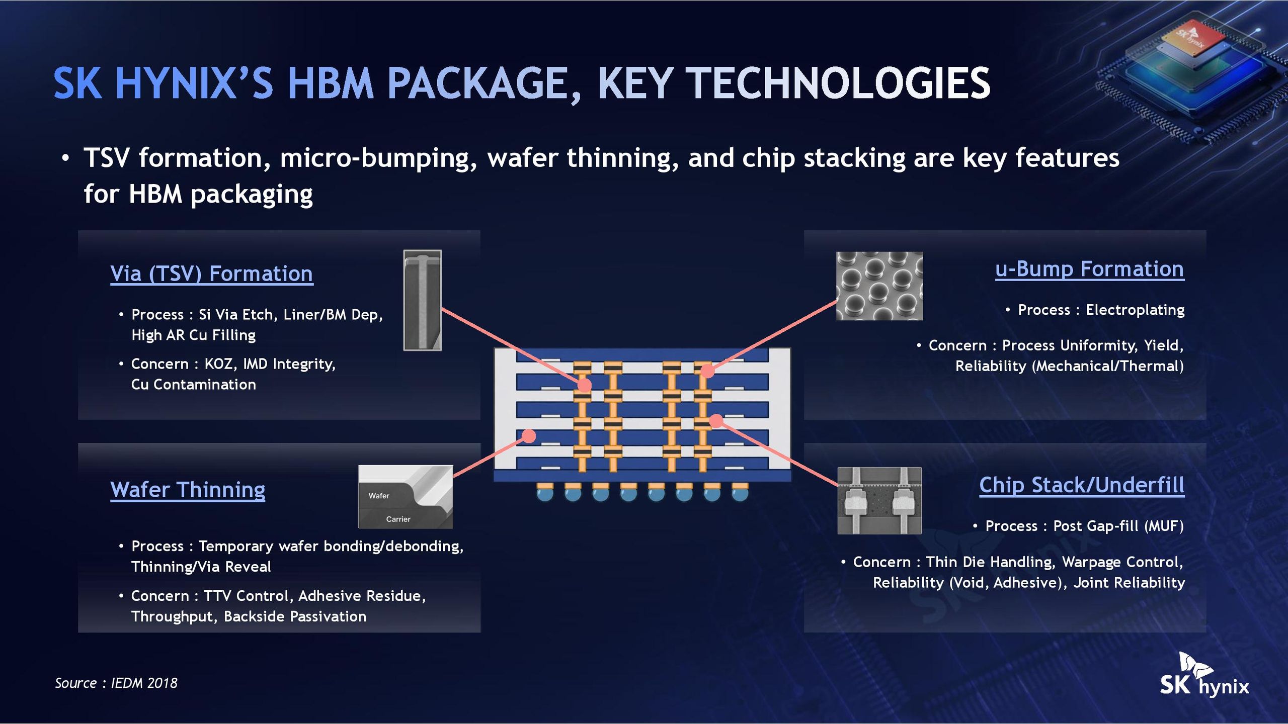
(Image credit: SK Hynix) (Image credit: SK Hynix) (Image credit: SK Hynix) (Image credit: SK Hynix) (Image credit: SK Hynix) (Image credit: SK Hynix) (Image credit: SK Hynix) (Image credit: SK Hynix) (Image credit: SK Hynix) (Image credit: SK Hynix) (Image credit: SK Hynix) (Image credit: SK Hynix) (Image credit: SK Hynix) (Image credit: SK Hynix) (Image credit: SK Hynix) (Image credit: SK Hynix) (Image credit: SK Hynix) (Image credit: SK Hynix) (Image credit: SK Hynix) (Image credit: SK Hynix) (Image credit: SK Hynix) (Image credit: SK Hynix) Image 1 of 22 View Original
TOPICS SK Hynix See all comments (0) Luke James Social Links Navigation Contributor Luke James is a freelance writer and journalist. Although his background is in legal, he has a personal interest in all things tech, especially hardware and microelectronics, and anything regulatory.
Key considerations
- Investor positioning can change fast
- Volatility remains possible near catalysts
- Macro rates and liquidity can dominate flows
Reference reading
- https://www.tomshardware.com/tech-industry/semiconductors/SPONSORED_LINK_URL
- https://www.tomshardware.com/tech-industry/semiconductors/sk-hynix-says-hybrid-bonding-wont-be-ready-for-hbm4e-as-ai-memory-runs-into-a-775-micron-ceiling#main
- https://www.tomshardware.com/my-account
- Microsoft Paint and Photos apps add invisible watermark to AI-generated content — developer reverse engineers GUID embedding
- Linux was announced by Linus Torvalds 35 years ago today — humble OS started with 10,000 lines of code but has now grown to 40 million, dominates global infrast
- China strategically slows exports of critical materials used in semiconductor fabrication to Taiwan — germanium and quartz exports to the region also threaten o
- LG's native 1,000 Hz 1080p gaming monitor has a matching $1,000 price tag — preorders open for the 25-inch UltraGear 25G590B
- Cooler Master Q300L v3 MicroATX case review: Sub-$45 MSRP offers incredible value for MicroATX chassis with included fans
Informational only. No financial advice. Do your own research.