
Inside optical and the battle for scale – how the AI industry is racing to integrate photonic interconnects
How optical interconnects and silicon photonics emerged as AI's next hot commodity
Near-packaged optics (NPO) gains ground as the industry hedges against CPO's growing pains
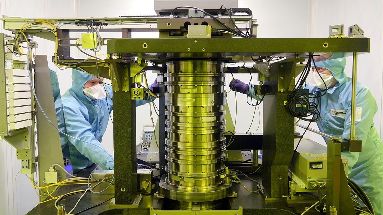
"The creation of a prototype of a domestically developed photolithography system designed for a 130nm process is an important milestone for Russia's microelectronics industry," Alexander Mikhailov, an analyst with Strategy Partners, told CNews. "It demonstrates that Russia has its own engineering expertise required to develop such equipment and paves the way for developing a range of systems targeting smaller process nodes (90nm and 65nm)."
Truth be told, while the Zelenograd-based ZNTC is responsible for the project, Belarus-based Planar was responsible for developing the lithography system, according to documents seen by CNews (which corroborates earlier reports ). In addition to the system itself, Planar was responsible for manufacturing mechanical assemblies and components, as well as commissioning the prototype. Lasers for the unit were developed by Lassard. Meanwhile, ZNTC is responsible for development of the overall system, design of the test and process equipment, projection-lens calculations, as well as process modeling and development, the report claims. Russia's Ministry of Industry and Trade allocated approximately $70 million for the entire development program.
It is estimated that one 130nm-capable ZNTC stepper costs $6.7 million, while its laser light source costs around $600,000, bringing the cost of a single tool to around $7.3 million. To put the number into context, ASML's PAS 5500/150 stepper had a list price of $3.1 million when it was launched in Q1 2001. Implying a cumulative inflation of about 88%, this translates to around $5.8 million in 2026 dollars. Meanwhile, the Russian stepper is a 200-mm machine capable of 130nm fabrication technologies.
Speaking of 130nm manufacturing processes — which Intel and AMD adopted in 2001 and 2002, respectively — Russian chipmakers have historically developed two 130nm-class nodes, but those technologies rely on lithography equipment from ASML. Whether or not ZNTC's stepper could be integrated into existing nodes remains unclear, but ZNTC claims that it is also responsible for process technology 'modeling and developing.' This likely refers to developing/qualifying the lithographic process around this particular machine —resist, exposure dose, focus/process window, masks, alignment/overlay, develop conditions, temperatures, etc. —rather than inventing an entire 130nm technology from scratch.
China's DUV technology 'at a similar stage to ASML in 2004,' analyst claims
Key considerations
- Investor positioning can change fast
- Volatility remains possible near catalysts
- Macro rates and liquidity can dominate flows
Reference reading
- https://www.tomshardware.com/tech-industry/semiconductors/SPONSORED_LINK_URL
- https://www.tomshardware.com/tech-industry/semiconductors/russias-zntc-reportedly-completes-development-of-130nm-capable-litho-tool-volume-production-still-years-away#main
- https://www.tomshardware.com/membership
- NVIDIA Isaac ROS 5.0 Advances Agentic, Open Source Robotics Development
- Black Friday laptop deals: What should small and medium-sized businesses be looking for?
- Data center construction spending hits record $85 billion annual pace
- Used PS5 Pros now cost $1,399 at GameStop, 50% more than new ones
- CD players are back, and offering up modern, interesting features
Informational only. No financial advice. Do your own research.