
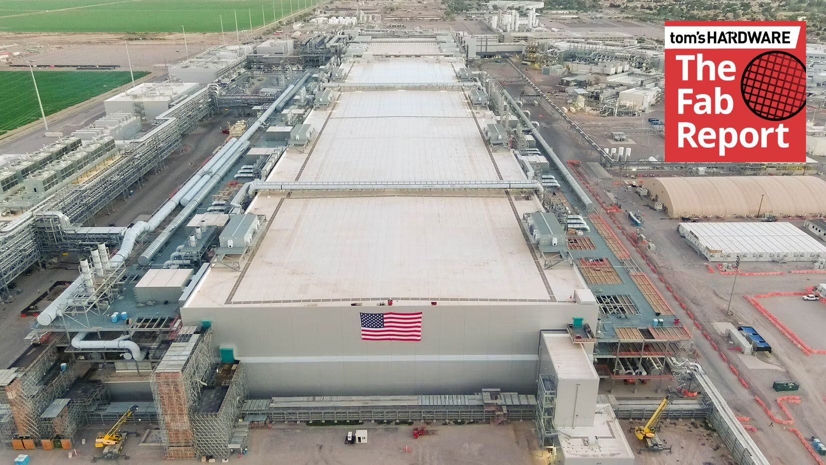
The Gordon Moore Park at Ronler Acres in Oregon is where Intel develops its most advanced logic process technologies and initiates volume production of the latest processors. Usage of High-NA EUV to produce select tiles for Panther Lake CPUs at D1X is a natural fit for the development fab, as it helps Intel to better understand how these lithography systems work. Meanwhile, it seems (though Intel has not explicitly confirmed) that, for now, High-NA EUV scanners are used to produce the same circuits as Low-NA EUV machines, so the use of next-generation lithography systems does not necessarily provide significant advantages over existing litho scanners.
Intel has also made progress with its 'Ohio One' manufacturing complex in New Albany, Ohio. Construction workers recently installed the first major structural truss at the site's first semiconductor fab, which represents a milestone in the development of the company's manufacturing operations in the state. The project is clearly an important part of Intel's long-term strategy to expand domestic production of chips using leading-edge process technologies for years to come.
Unfortunately, Intel did not provide an updated construction schedule for Ohio One or disclose when the first fab is expected to begin operations. Intel also did not reveal which process technology the facility will eventually use or the estimated manufacturing capacity it will provide. Therefore, while construction continues, which is good news, the announcement does not clarify exactly when Ohio One will contribute to Intel's output.
Intel closes out RAMP-C production pilot that paid Nvidia and others to run test chips on 18A
TSMC, Samsung, and Intel shore up support with ASML to deploy larger High-NA EUV photomasks
Elon Musk's Terafab will reportedly receive its first EUV tool from ASML in mid-2027
In addition to leading-edge manufacturing capacity in the U.S., Intel continues to invest in advanced packaging technologies. Oregon serves as the company's main research and development center for advanced logic and 3D interconnect technologies, while Arizona hosts advanced packaging R&D, assembly, and testing operations. Intel uses its site in New Mexico to produce its complex multi-chiplet processors relying on advanced packaging methods — starting with modest EMIB and all the way to next-generation EMIB-T and Foveros technologies.
Also, Intel recently broke ground on a new photomask manufacturing facility in Santa Clara, California. The new facility will be an important part of Intel's supply chain in the U.S., as the company will be the only chipmaker in America to develop and produce chips using leading-edge nodes completely in the U.S. (both Samsung and TSMC currently lack leading-edge process R&D in America; they do not run their own photomask shops in the U.S., and Samsung has abandoned its plan to build an advanced packaging facility in Texas). Of course, Intel critically depends on tools from Europe and materials from Japan, but even as its major rivals invest hundreds of billions in their U.S. production capacity, Intel remains ahead.
To highlight its American supply chain, Intel disclosed that its U.S. operations involve more than 4,500 suppliers across 49 states, as its annual domestic expenditures exceed $29 billion. The company stressed that domestic semiconductor leadership requires not only wafer fabrication capacity but also research, process development, advanced packaging, and a comprehensive supply chain.
Follow Tom's Hardware on Google News , or add us as a preferred source , to get our latest news, analysis, & reviews in your feeds.
Anton Shilov Social Links Navigation Contributing Writer Anton Shilov is a contributing writer at Tom’s Hardware. Over the past couple of decades, he has covered everything from CPUs and GPUs to supercomputers and from modern process technologies and latest fab tools to high-tech industry trends.
Key considerations
- Investor positioning can change fast
- Volatility remains possible near catalysts
- Macro rates and liquidity can dominate flows
Reference reading
- https://www.tomshardware.com/tech-industry/semiconductors/SPONSORED_LINK_URL
- https://www.tomshardware.com/tech-industry/semiconductors/intel-installs-production-tools-at-fab-62-in-arizona-provides-updates-on-ohio-chip-fab-confirms-high-na-euv-for-high-volume-manufacturing-in-2028#main
- https://www.tomshardware.com/membership
- Cloud Deployment Incoming: ‘Call of Duty: Modern Warfare 4’ Arrives on GeForce NOW
- Rare archival footage tours the CompUSA NYC store in November 2000
- NVIDIA Cloud Partners Scale Across Europe — Sovereign, Open and Built for Safe AI Agents
- Russia deploys 3D-printed cruise missiles with US electronics in Ukraine, can hit 500mph with a 745-mile range
- UK proposes 14-year prison sentences for undersea cable saboteurs amid Russian trawler threats
Informational only. No financial advice. Do your own research.