
When you purchase through links on our site, we may earn an affiliate commission. Here’s how it works .
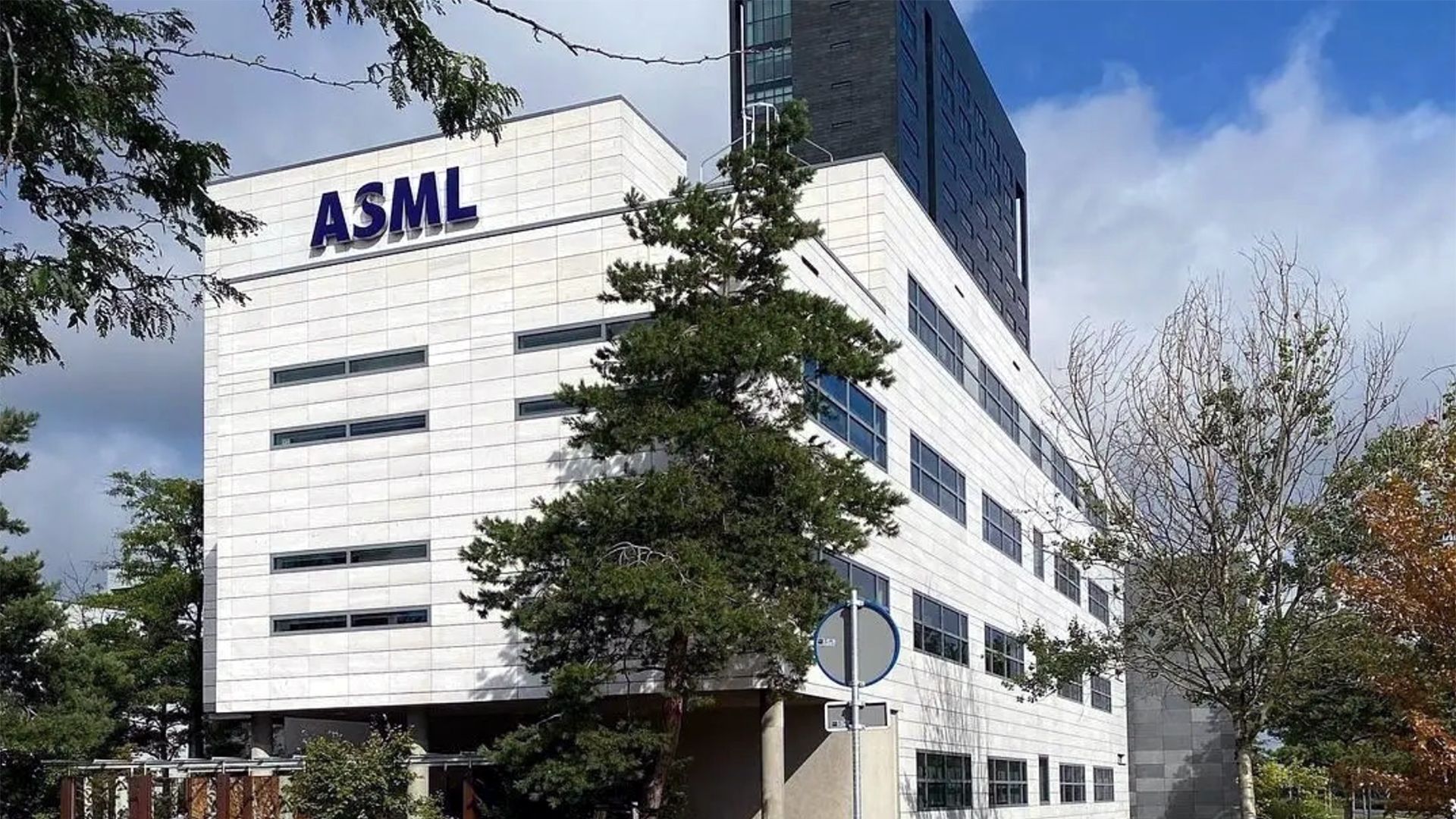
Modern EUV lithography systems use laser-produced plasma light sources that fire powerful CO₂ laser pulses at tiny droplets of molten tin, around 30 microns in diameter, which turns them into ionized plasma with electron temperatures of several tens of electron volts that emits 13.5-nm EUV radiation. The light is then collected by a roughly 0.5-meter elliptical collector mirror coated with multiple layers of molybdenum and silicon, which selectively reflects as much 13.5-nm radiation as possible and directs it toward the intermediate focus at the entrance to the scanner. Since virtually all materials absorb EUV radiation — even specialized multilayer mirrors absorb a substantial portion of it — the entire optical path must operate in vacuum and use reflective rather than conventional refractive optics, which is one reason why generating sufficient EUV source power remains challenging.
Despite major challenges, ASML has gradually increased the source power of its LPP light sources from around 250W to around 500W and plans to increase it to 1000W in the coming years. In addition, the company plans to almost double the number of generated tin droplets to 100,000 every second.
A free-electron laser (FEL) generates EUV light by accelerating electrons to nearly the speed of light and passing the electron beam through an undulator, a series of alternating magnets that force electrons to oscillate and emit radiation. Interaction between the electrons and their radiation causes them to form microscopic bunches and emit light with a 13.5-nm wavelength. This approach eliminates tin droplets and associated debris (that require usage of protective pellicles on photomasks) as well as potentially provides substantially higher EUV power than LPP sources. Furthermore, one FEL can potentially replace multiple LPP sources with a single FEL and a large EUV beam-distribution system.
Yet, there is a major tradeoff: instead of a relatively compact LPP, FEL requires a highly complex particle accelerator, an electron source, a long undulator, electron-beam control, radiation shielding, and an extremely complex distribution system featuring mirrors capable of handling and distributing very high EUV power without losing too much of it along the way. The whole machine must achieve semiconductor fab levels of availability, efficiency, and cost, something that took ASML and the rest of the industry years to achieve.
China's DUV technology 'at a similar stage to ASML in 2004,' analyst claims
Key considerations
- Investor positioning can change fast
- Volatility remains possible near catalysts
- Macro rates and liquidity can dominate flows
Reference reading
- https://www.tomshardware.com/tech-industry/semiconductors/SPONSORED_LINK_URL
- https://www.tomshardware.com/tech-industry/semiconductors/asml-snubs-elon-musk-backed-particle-accelerator-chipmaking-tech-firm-doubles-down-on-1-000w-laser-produced-plasma-systems-for-chipmaking-tools#main
- https://www.tomshardware.com/membership
- Pick up a giant 18-inch RTX 5080-powered Asus gaming laptop from Best Buy and save $600 — the ROG Strix G18 also comes with 32GB of memory and a 2TB SSD
- Skild AI Taps NVIDIA Physical AI to Teach Robots New Tasks From a Single Video
- Developer vibe codes a tool to let Nvidia RTX 50-series laptop owners crank up their power limits — can juice RTX 5090 mobile GPU to 225W
- From Megawatts to Tokens: How NVIDIA Maximizes AI Factory Production
- University of Manchester Uses NVIDIA Earth-2 to Forecast Air Pollution Across the UK
Informational only. No financial advice. Do your own research.