
When you purchase through links on our site, we may earn an affiliate commission. Here’s how it works .
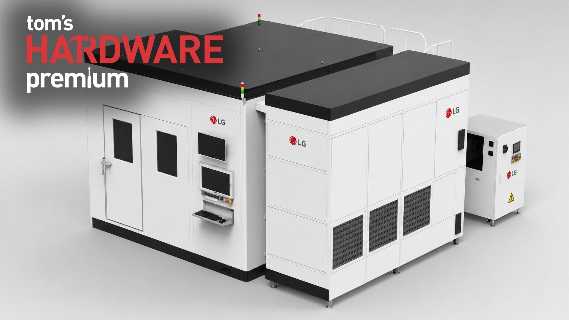
LG-PRI's Laser Direct Imaging (LDI) system is a maskless lithography machine designed to pattern fine metal interconnects for advanced semiconductor packaging. While the company has developed various versions of the machine, its highest-resolution version can produce 1.5-µm line-and-space (L/S) patterns, which should be fine to 'print' wiring pitches of about 3 µm. The production equipment uses a 405-nm laser-diode light source and can process substrates as large as 600 × 600 mm, according to various media reports.
LG positions its LDI system primarily for advanced semiconductor packaging using organic and then glass substrates, displays, and MEMS. Yet, it can also be used to build high-density printed circuit boards (PCBs) for mobile devices or prototype purposes.
LG is entering an already established direct-imaging market led by KLA, Screen Holdings, Limata, and ORC, but participated in by a dozen manufacturers from Germany, France, Switzerland, Japan, and even China. What is notable is that LG is offering LDI systems with line/space capability down to 1.5-µm, which means it is targeting the higher end of the market. Yet, to establish a position, LG plans to price its LDI system competitively.
There are many ways to pattern substrates, including photolithography, e-beam lithography, nanoimprint lithography , and laser direct imaging, just to name a few. LDI is a maskless lithography process in which a laser exposes a digitally generated circuit pattern directly onto a photoresist-coated substrate, rather than transferring the pattern through a physical photomask . Instead of a photomask, an LDI system uses a digitally controlled pattern generator and projection optics, which resembles how a laser cinema projector projects a digital image onto a screen, except that LDI projects a circuit pattern onto photoresist. After development, the exposed resist leaves a pattern that defines where metal interconnects will be formed in later processing steps.
Intel's EMIB packaging gains traction as chip designers look beyond TSMC's constrained CoWoS
TSMC says panel packaging won't replace CoWoS anytime soon for the largest future AI processors
Chinese startup claims photonic chip production without DUV lithography, says nanoimprint process cuts costs by 90%
LG's LDI machine can produce down to 1.5-µm line-and-space patterns, which is good enough for chip substrates and even redistribution layers ( TSMC CoWoS-R/-L uses RDL interposers with a minimum 4-µm pitch, or 2-µm line width/spacing). In contrast, competing products offer 1-µm, 3-µm, and 5-µm versions for different applications. While LDI in general cannot boast the resolutions offered by modern DUV, EUV , or e-beam lithography machines, LDI trades ultimate resolution for vastly higher throughput and large-area processing, exactly what the doctor ordered for production of PCBs or chip packaging. With current-generation LDI, the RDL interposer is the most advanced thing that these devices can pattern, as both CoWoS-S and CoWoS-L/EMIB-like technologies require considerably higher resolution. Meanwhile, there is another advantage that LDI machines have over lithography systems that rely on photomasks.
Because the image is generated digitally, the system can create and calibrate patterns in real time, while projection optics, precision alignment, and stage control position the pattern accurately on the substrate. This capability is important because the dimensions/geometry of packaging substrates can vary and because organic substrates can expand, contract, or warp during processing. Given that we are talking about a 1.5-µm-scale wiring pattern, any shift from the nominal layout may result in a solder bridge or a faulty contact, which means yield loss. That said, the ability to adjust the pattern to the peculiarities of a substrate may be a game-changer for OSATs, their customers, and a major selling point for devices that can do it.
Unlike competing chaebols Samsung and SK Group, LG Group does not produce chips, even though its divisions supply various materials and components for the semiconductor industry. To that end, it is perfectly reasonable for the company to enter the market for tools for the production of chip packages or PCBs.
In fact, LG PRI is not entering the exposure-equipment business from scratch. PRI traces its history to the Goldstar Production Technology Research Institute, established in 1987, and has worked on manufacturing and productivity technologies covering semiconductors, displays, and rechargeable batteries. Specifically, LG had already commercialized LDI technology for display manufacturing and supplied such equipment to LG Display.
As a result, the semiconductor packaging-grade equipment represents an expansion of an existing LG technology into a new market rather than the development of an entirely new exposure platform from scratch and without any experience. Interestingly, LDI is the first element of LG's semiconductor equipment ambitions. The company reportedly plans to expand its portfolio into high-bandwidth memory (HBM) inspection equipment as well as through-glass-via (TGV) laser systems for glass substrates.
Before LG expands to inspection or laser drilling tools, it will have to establish itself as a producer of reliable tools used for chip packaging, which will likely take years. For now, the significance of the deal with the undisclosed OSAT is less about business and more about the fact that an OSAT decided to give LG's LDI machine a try. Moving from university R&D installations to an OSAT mass-production facility provides LG a starting point for pursuing additional external orders.
Whether LG can establish itself alongside Applied Materials, ORC, or Screen will depend on how its equipment performs in production and whether its emphasis on competitive pricing proves sufficient to persuade more packaging companies to adopt the system.
In any case, a new Wafer Fab Equipment player is here, which is good news considering shortages of virtually all chipmaking tools. While LG's entrance will hardly have any noticeable impact on the market for at least a couple of years, another supplier could eventually add much-needed capacity, increase competition, and give chipmakers and OSATs another source of advanced packaging equipment.
Anton Shilov is a contributing writer at Tom\u2019s Hardware. Over the past couple of decades, he has covered everything from CPUs and GPUs to supercomputers and from modern process technologies and latest fab tools to high-tech industry trends. ","collapsible":{"enabled":true,"maxHeight":250,"readMoreText":"Read more","readLessText":"Read less"}}), "https://slice.vanilla.futurecdn.net/13-4-25/js/authorBio.js"); } else { console.error('%c FTE ','background: #9306F9; color: #ffffff','no lazy slice hydration function available'); } Anton Shilov Social Links Navigation Contributing Writer Anton Shilov is a contributing writer at Tom’s Hardware. Over the past couple of decades, he has covered everything from CPUs and GPUs to supercomputers and from modern process technologies and latest fab tools to high-tech industry trends.
Key considerations
- Investor positioning can change fast
- Volatility remains possible near catalysts
- Macro rates and liquidity can dominate flows
Reference reading
- https://www.tomshardware.com/tech-industry/semiconductors/SPONSORED_LINK_URL
- https://www.tomshardware.com/tech-industry/semiconductors/lg-enters-chip-packaging-arena-with-laser-direct-imaging-machine-as-tsmcs-cowos-remains-constrained-maskless-machine-is-designed-to-pattern-fine-interconnects-trading-resolution-for-higher-throughput#main
- https://www.tomshardware.com/my-account
- Nvidia’s GB300-powered DGX Station desktop tower listed for nearly $100,000 online — Enterprise AI powerhouse now available to buy for mere mortals with lots of
- Save $532 on a 480 Hz OLED gaming monitor — Amazon drops a massive 53% discount on the LG UltraGear 27GX790A-B
- The world's first webcam was switched off 25 years ago today — 128×128 grayscale feed predated the World Wide Web to monitor a Cambridge coffee pot
- Asus ROG Strix XG32UQWMS 4K OLED gaming monitor review: Fast and flexible performance
- CPU-Z gets biggest update since 2001 with V3 — 100+ health checks, built-in stress testing, and XOC effective clock tracking
Informational only. No financial advice. Do your own research.